
PCB Trace Repair Kit Soldering Lugs
3.4Editor score
2,780-piece repair package
Purple copper construction
Fixed-pin solder components
Discover the best PCB Trace Repair Kit options by comparing copper pads, repair sheets, solder masks, enameled wire, precision, and application coverage.
A PCB trace repair kit helps technicians restore damaged copper paths, lifted solder points, and broken board connections without replacing an entire circuit board. The best kit depends on the repair type, component scale, material compatibility, and the level of precision your electronics work demands.
We compared all ten products by examining their stated construction, package contents, repair applications, conductivity, placement features, and suitability for phones, computers, motherboards, and general electronics. The list includes copper soldering-dot sheets, fine enameled wire, a solder-mask repair set, and compact rework-pad systems.
Each review highlights the product's most useful qualities and practical limitations, helping you identify the right option for your repair bench. Product details and availability can change, and prices fluctuate over time, so verify the current listing before purchasing.
3.4Editor score

5.0Editor score

4.2Editor score
The comparison below places all ten kits side by side, focusing on repair format, materials, included components, precision, and suitable circuit-board applications.
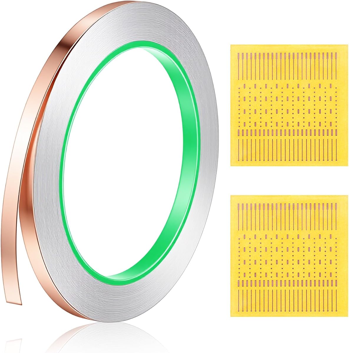

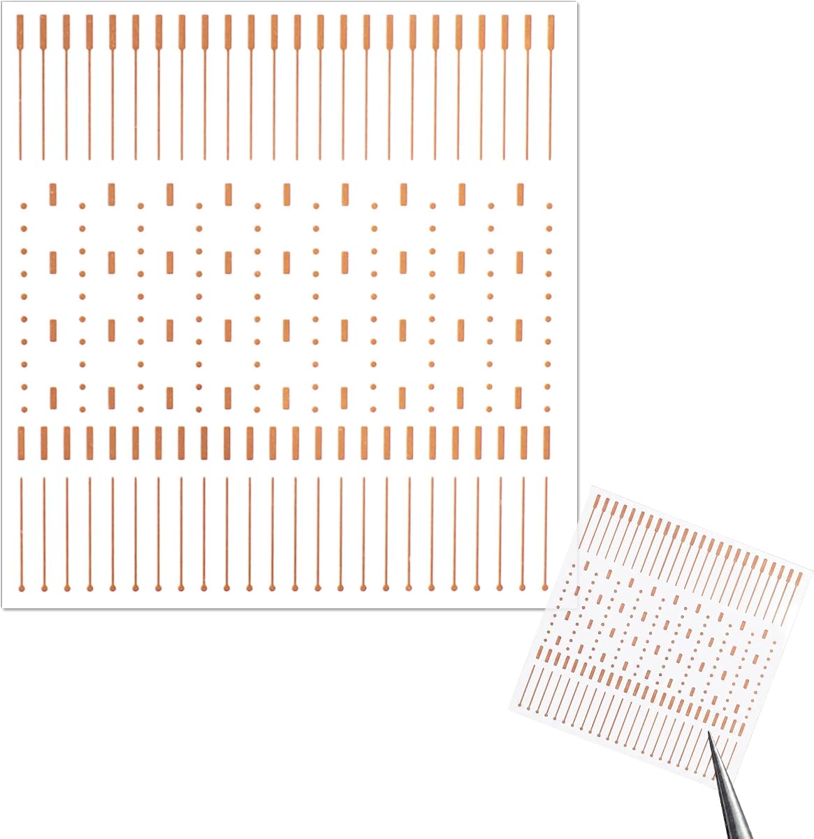


This PCB Trace Repair Kit Soldering Lugs set is built around a notably complete package of 2,780 soldering pads, solder blocks, and related repair components. Its stated 3.4 rating reflects a mixed customer reception, but the product data distinguishes it through sheer quantity and a focus on efficient, repeatable board restoration. It is positioned as a general bench supply rather than a single-purpose patch sheet.
We may earn a commission when you buy through this link, at no additional cost to you.
The individual components are described as purple copper, providing the electrical conductivity and durability needed for spot welding, auxiliary welding, and conventional circuit-board repairs. Fixed pins are another useful feature because they help hold each component in position during soldering. That stability can make placement more consistent than working with loose conductive material, especially on crowded motherboards where there is little room to maneuver.
The main trade-off is the modest rating and the fact that such a large assortment may overwhelm a new technician. Buyers should organize the pieces by type and size before use, and they should confirm that the included components match the dimensions of the damaged pads being restored. The listed design is appealing for users who expect to make many repairs or want a broad supply rather than a limited specialty kit.
This is a sensible choice for repair shops, advanced hobbyists, and mobile-device technicians who want abundant consumables on hand. It may be less suitable for someone needing only one delicate bridge on a small board, but its large assortment offers useful coverage for a variety of PCB trace and solder-point tasks.
The 2,780-piece count is the strongest feature for frequent users, reducing the likelihood of running out of common pads during repeated repair sessions. Sorting the assortment into dedicated containers can make the broad selection easier to manage.
Retaining pins are designed to keep components secure while heat is applied, which is useful on dense boards where accurate placement is essential. This feature supports cleaner, more controlled soldering than unsecured loose pieces.
We may earn a commission when you buy through this link, at no additional cost to you.
The Amaxiu PCB Trace Repair Kit is a two-sheet system containing 208 spots per sheet and 624 dots in total. Each sheet is described as 6.3 millimeters wide and 20 meters long, while the pre-cut copper-and-tin dots are intended for bridging damaged or missing connections. No numerical customer rating is supplied, so the available evidence rests on the stated construction and intended applications.
We may earn a commission when you buy through this link, at no additional cost to you.
Its principal strength is the combination of organized storage and fine-point versatility. The copper foil and tin construction is presented as electrically conductive and heat resistant, allowing repeated use when handling broken traces and damaged pads. Pre-cut dots can be placed directly at the defect, while the reinforced retaining-pin structure is designed to reduce reliance on longer flying-wire techniques.
That precision comes with a learning curve. The 6.3-millimeter format and emphasis on very small solder joints make the kit more relevant to experienced microsoldering work than casual electronics projects. Users should also inspect the product listing to confirm the physical arrangement and quantity because the numerical rating is unavailable and detailed buyer feedback cannot be evaluated here.
The Amaxiu kit is a strong option for motherboard repairers, phone specialists, and users who regularly bridge fine-pitch points. It offers a generous number of repair spots, clean organization, and a stated no-trace workflow, making it particularly useful when a repair bench needs more than a handful of sacrificial jumpers.
Using pre-cut conductive dots avoids manually shaping every repair point. This can speed routine motherboard jumpers and make it easier to match the scale of a damaged pad or isolated trace.
Long tape sheets allow unused dots to remain attached and easy to locate. The format is convenient for technicians who want multiple options on the bench without sorting hundreds of individually loose parts.
We may earn a commission when you buy through this link, at no additional cost to you.
The Amabro PCB Trace Repair Kit uses a focused package of two repair patches and one pair of stainless steel tweezers. The patches measure 3 by 2.8 centimeters, while the tweezers are 13.6 centimeters long with a 1-millimeter tip. Because no numerical rating is available, the product should be evaluated from its stated materials, included accessories, and suitability for common board-level work.
We may earn a commission when you buy through this link, at no additional cost to you.
The tweezers are a particularly relevant addition for microsoldering. A narrow tip gives the technician more control when handling tiny dots or positioning a patch on a crowded circuit board. The patches are made from tin sheet, which the listing says provides stable conductivity and heat resistance, while the tweezers offer a firm grip and antistatic construction.
The flat patch layout is designed to transfer heat evenly and blend into the board after soldering. It can be used for spot welding, auxiliary soldering, damaged traces, and broken pads across phones, tablets, laptops, and other electronics. Compatibility with soldering irons, hot-air stations, and common welding accessories adds flexibility, although the two-patch quantity is smaller than the several-hundred-dot sheet kits.
This package is best for a technician who values a compact, organized setup and appreciates having fine-tip tweezers supplied with the consumables. It is a practical alternative for occasional repairs where hundreds of pre-cut spots are unnecessary, but it offers less material variety than the larger copper-dot kits in this comparison.
The included 1-millimeter tip helps position tiny conductive pieces without disturbing nearby components. This makes the package more complete for immediate bench use at a finer level of repair.
Thin tin patches are intended to sit close to the board surface, which can help preserve clearance around compact phone and tablet assemblies. Their stated no-residue design also supports a neat final appearance.
We may earn a commission when you buy through this link, at no additional cost to you.
The Solder Piece No-Trace Auxiliary Welding kit offers a single sheet containing 208 repair spots in different shapes and sizes. The sheet is only 1.11 inches long, making this a compact option for mobile-device precision work. No customer rating is provided, but the product information clearly positions it as a solder-dot system for restoring missing solder points and bridging broken circuit paths.
We may earn a commission when you buy through this link, at no additional cost to you.
Its red copper construction is intended to provide fast heat transfer and stable electrical performance. Because the sheet contains varied geometries, a technician can select a dot that better matches the scale and outline of a damaged pad. The flat structure is also designed to keep the repaired board neat, and the dots can be used with standard soldering equipment for auxiliary or spot welding.
The main limitation is the single-sheet package. Although 208 spots are available, users with a heavy workload may eventually want additional sheets or a more comprehensive assortment. The absence of customer feedback also makes it harder to judge long-term consistency, so the stated features should be checked against the actual repair tasks performed on your bench.
This kit is a good match for experienced hobbyists and phone-repair technicians who need a portable range of copper points for fine traces. Its varied shapes and compact dimensions make it particularly useful when a single damaged location must be matched accurately without carrying a much larger repair system.
A selection of spot dimensions gives the repair technician more flexibility when dealing with peeling pads, narrow traces, or irregular connection points. Matching the geometry to the defect can improve placement accuracy.
The small sheet is easy to carry between workspaces and uses little bench space. It also allows only the required portion of the repair-dot sheet to remain in the immediate work area.
We may earn a commission when you buy through this link, at no additional cost to you.
The Soldering Lugs Rework Pad is aimed at professional-level phone IC, motherboard, and BGA pad restoration. Its 4.2 rating is among the stronger numerical ratings in this group, and the product is distinguished by premium copper construction, reinforced retaining pins, and a flat application surface designed to reduce virtual-welding problems caused by uneven placement.
We may earn a commission when you buy through this link, at no additional cost to you.
The main benefit is stability. Retaining pins keep the rework pad in position while heat is applied, allowing the technician to concentrate on the solder joint rather than continuously holding a tiny component against a crowded board. Its stated jump-wire function adds another layer of usefulness, making it appropriate for motherboard jumper tasks, microsoldering, fingerprint-welding locations, and broader PCB trace work.
This is not the simplest consumable for a complete beginner. Applying the pad correctly requires careful preparation, alignment, and control of heat, and the product data provides less detail about the number and geometry of included points than some competing sheet kits. A premium designation should therefore refer to the stated construction and specialized application rather than an assumption that it performs every task better.
It is a strong recommendation for experienced repair technicians who regularly work on BGA packages, phone ICs, and fine motherboard traces. Buyers who value a stable, flat, purpose-built rework surface are likely to appreciate this kit more than a general user seeking a simple collection of loose copper points.
A level surface helps the repair material remain in consistent contact with the board. The listing specifically links this stability to fewer virtual-welding issues and cleaner, more reliable joints.
BGA restoration, IC-pad work, and fine motherboard jumpers are the kit's strongest use cases. Technicians with appropriate soldering equipment can use it as a focused solution for especially small connection points.
We may earn a commission when you buy through this link, at no additional cost to you.
The 5pcs Enameled Copper Wire kit is a different kind of PCB repair solution: instead of pre-cut pads, it supplies five spools of fine wire for creating jumpers and restoring connections manually. The 0.1-millimeter diameter and 12-meter length per spool make it well suited to precision motherboard work, while its 4.5 rating is the second-highest numerical score among the products listed.
We may earn a commission when you buy through this link, at no additional cost to you.
The enamel coating is designed to be directly solderable without first scraping away the insulation. That convenience saves preparation time and helps the wire retain its precise shape while being routed around nearby components. High-conductivity copper is intended to support dependable electrical performance, and the generous length gives home users or shops considerable material for numerous small repairs.
Wire requires more manual shaping than a fixed pad or solder dot, and very fine routes can be difficult for inexperienced hands. The repair outcome also depends heavily on insulation clearance, solder temperature, and the technician's ability to secure the conductor without creating a short. A multimeter and careful visual inspection remain important after the joint cools.
This product is ideal when a damaged trace needs a custom route between two points that cannot be connected efficiently with a pre-cut spot. It is especially useful for phone, computer, and laptop motherboard maintenance, provided the user has steady soldering control and understands how to route fine enameled wire safely.
Because the coating can be soldered directly, the wire does not need to be stripped before use. This shortens the workflow and helps preserve the fine diameter during handling.
Sixty meters of combined wire provide ample material for multiple jumpers and unusual board geometries. Custom routes can connect distant or awkwardly positioned test points while maintaining a small physical footprint.
We may earn a commission when you buy through this link, at no additional cost to you.
The SHENLIU PCB Trace Repair Kit combines two 1.1-inch by 1.1-inch sheets containing 416 individual red-copper dots. Its perfect 5.0 numerical rating makes it the most highly rated option in this guide, while the product data emphasizes genuine red copper, rapid heat transfer, organized storage, and a no-trace repair process.
We may earn a commission when you buy through this link, at no additional cost to you.
The format balances quantity with compactness. Each sheet holds 208 dots, providing a substantial supply without requiring the enormous assortment offered by the 2,780-piece budget kit. Flat dots are designed for accurate placement on damaged pads, and their structure turns a difficult jumper-wire task into a more controlled positioning and heating procedure. The stated use with spot welders or standard pad-based methods also broadens compatibility.
Users must still understand the difference between applying a copper repair point and simply flooding the board with solder. Heat control, flux use, and verification of the intended circuit are important. Copper does not create a valid connection by itself, so the dot must be soldered to the correct trace or pad and checked for continuity and unintended shorts.
For experienced phone, tablet, and laptop repairers, this is the most balanced all-around choice in the list. It offers a strong customer rating, enough material for repeated jobs, and a clean organized format, making it a particularly practical selection for a technician who wants more capability than a two-patch set without an enormous loose-component inventory.
Two compact sheets hold 416 points, offering a substantial working supply while remaining easy to store. This makes the format practical for technicians who want consistency without a crowded collection of individual parts.
The stated red-copper material is intended to transfer heat rapidly and uniformly. That property can help technicians place and solder a repair point efficiently when working around fine-pitch board features.
We may earn a commission when you buy through this link, at no additional cost to you.
The PCB Trace Repair Kit Soldering Block provides 208 copper soldering pads in a straightforward format for PCB restoration. Its 4.0 rating indicates solid customer reception, and the product information emphasizes reliable conductivity, precise placement, smooth heat transfer, and a no-trace design intended to leave the repaired board visually clean.
We may earn a commission when you buy through this link, at no additional cost to you.
Its 208-piece count is enough for a meaningful number of repairs, while the absence of dozens of other component types keeps the package understandable. Each pad is designed to be positioned at a damaged solder point and heated, restoring conductivity between the remaining copper and the repair location. The stated no-mark result is particularly relevant to visible areas and compact electronic assemblies where cosmetic quality matters.
The product listing does not specify individual pad dimensions or describe a broader accessory set, so buyers may need to inspect the product images carefully to confirm scale. As with any solder-dot system, the final connection still depends on correct identification of the damaged trace, adequate flux, controlled heat, and a continuity check.
This is a balanced selection for mobile-phone technicians, electronics hobbyists, and general repair benches that need a single type of copper consumable. Its straightforward packaging and solid rating make it easier to recommend than a more specialized multi-function system, particularly for users who do not need hundreds of different components.
Knowing that the kit includes 208 pads makes consumable planning easier. A single-product format also makes it straightforward to identify the correct refill or replacement when the original sheet is depleted.
The listing emphasizes smooth heat transfer and precise placement, both of which are important for creating a low-profile repair. These qualities can help reduce excess solder around sensitive neighboring components.
We may earn a commission when you buy through this link, at no additional cost to you.
The PCB Circuit Board Solder Mask Repair Kit is intended for a different type of board damage than most copper-dot products. It is designed for peeling or locally damaged solder-mask layers on computer and mobile-phone circuit boards, and its package includes a flashlight and green oil described as useful accessories for BGA soldering.
We may earn a commission when you buy through this link, at no additional cost to you.
The green oil is likely the most distinctive element in the set, offering a liquid compound that can assist in the mask-repair process. The flashlight improves visibility around densely populated board areas and during detailed inspection, while the stencils included in the broader package can be used in conjunction with flux. The listing recommends coating stencils with flux to prevent solder-mask ink from adhering to them.
Its 3.0 rating is the lowest numerical score in the comparison, and the listing gives fewer details than several copper-pad kits. Product information also varies between a three-type optional package and the specific tools highlighted in the description. Buyers should carefully verify the final package contents, especially if a specific accessory is required for their intended process.
This kit is worth considering when the problem is a missing, scratched, or peeling protective surface rather than a completely severed copper trace. It can complement a conventional PCB trace repair kit, but it should not be treated as a direct substitute for copper jumpers, solder dots, or fine wire. Confirm that the surface-repair approach matches the board's layer structure before use.
Solder-mask repair becomes relevant when a board's protective coating is locally damaged or lifting. This set addresses that surface issue rather than replacing missing copper connectivity.
The included flashlight can help reveal small cracks, residue, or exposed areas around dense components. Clearer inspection is especially valuable before and after applying a cosmetic or protective repair layer.
We may earn a commission when you buy through this link, at no additional cost to you.
The Soldering Lugs Solder Piece uses a copper-wire repair pad mounted on a plastic plate to create more than 100 solder points in different shapes. Its 3.4 rating places it in the middle of this comparison, while the compact 4.8-by-5.8-centimeter footprint and peel-and-apply design distinguish it from loose dot sheets and flexible jumper wire.
We may earn a commission when you buy through this link, at no additional cost to you.
The multiple-point layout gives technicians a broad selection for phone IC, touch-board, fingerprint-welding, BGA-PCB, and flying-wire tasks. Reinforced retaining pins are intended to keep the pad stable during soldering, while the flat surface is designed to avoid uneven-contact problems. Because the points remain organized on a backing plate, the kit may be easier to handle than hundreds of loose components.
The fixed plate does impose some limitations. It cannot be reshaped as freely as fine wire, and the product's 3.4 rating suggests that customer experiences are not uniformly positive. The prepared backing may also add bulk compared with a flat copper sheet, although the stated dimensions remain compact for a workbench.
This product is most useful for mobile-device and motherboard technicians who want multiple soldering points available from a convenient, unified pad. It is a practical alternative for users who prefer organized, ready-positioned repair points but do not need a full sheet of individually separated solder dots.
More than 100 points in different forms allow a technician to select a suitable repair geometry for varied solder locations. Keeping the points on one plate can make the bench faster and less cluttered.
Removing the protective layer prepares the pad for immediate placement. This quick setup helps minimize delay before soldering and supports a controlled repair workflow.
We may earn a commission when you buy through this link, at no additional cost to you.
The right PCB trace repair kit depends on the type of board damage, the available soldering equipment, the required repair scale, and whether you need copper pads, jumper wire, or solder-mask materials.
A missing copper trace or lifted solder pad calls for a conductive bridge, while a loose jumper may be better handled with fine enameled wire. A damaged or peeling solder-mask layer requires a surface-repair product rather than a copper-dot sheet. Begin by inspecting the board and determining whether the fault involves conductivity, a mounting point, the protective coating, or a combination of issues. Matching the product format to the defect prevents a technically capable kit from being used in a way that adds unnecessary complexity.
Choose copper pads for missing or broken connection points, wire for custom routing, and solder-mask materials for exposed or damaged surface layers. Diagnostic tools such as a multimeter should confirm the fault before any heat is applied.
Pre-cut solder dots are convenient for repeatable repairs because they arrive in organized positions and can be placed directly over a defect. Large multi-point pads reduce clutter, while loose sheets offer many individual shapes. Fine wire is the most flexible option for reaching distant or irregular points but demands more routing skill. A multi-piece set can be convenient for a general bench, whereas a small patch-and-tweezer package is easier to manage for occasional work.
Think about workflow rather than quantity alone. Choose a format that matches the size, density, and geometry of the boards you regularly service.
Copper and copper-tin combinations are commonly used because they conduct heat and electricity effectively. Tin sheet is another listed option for patch-style repairs. The important point is that the repair material must form a sound electrical path with the board's original copper and remain stable under soldering temperatures. Product descriptions that specify conductivity, heat resistance, and exact materials provide a more useful basis for comparison than broad durability claims alone.
For electrically critical work, inspect the finished joint and test continuity after it cools. No material compensates for a poorly prepared or incorrectly located connection.
Precision kits are designed for soldering irons, hot-air stations, and sometimes spot welders, but the ideal tool depends on the board. A flat, stable repair point is useful only if heat can be applied evenly without cooking nearby parts. Larger solder masses retain more heat than fine wire, so operators must balance speed against the risk of lifting adjacent pads or disturbing sensitive components. Any stated no-trace or no-residue result also assumes proper technique rather than automatic results.
Use the lowest effective heat, apply flux suited to the board, and move promptly if a component begins to move. Practice on a damaged donor board before attempting a valuable device.
Fine phone motherboards and BGA areas require more than a large, loosely placed repair point. Look for flat geometry, reinforced retaining pins, pre-cut shapes, or an included narrow-tip tweezer. These features can reduce movement during soldering and help the conductive material remain centered. A no-trace design is also valuable when cosmetic damage would be conspicuous or when a raised repair could interfere with an enclosure or nearby component.
Precision is more important than sheer quantity on small electronics. Choose a smaller point when a large one crowds the defect or cannot contact the intended trace.
Useful accessories can make a repair consumable more complete. The Amabro set includes stainless steel tweezers with a narrow tip, while the solder-mask kit includes green oil and an inspection flashlight. Accessories such as flux, solder, and cleaning materials may still be needed separately, so check what is actually included before planning a repair. A larger assortment may save trips to the supply shelf, but it can also be harder to organize.
Prioritize accessories that directly support the repair method. Tweezers are especially relevant for tiny dots, while illumination and surface compounds are more valuable for mask-layer work.
Most products in this guide are described for phones, tablets, laptops, motherboards, TVs, keyboards, and general circuit boards, but the formats are not equally suited to every device. A high-density phone board calls for finer points and careful heat control, while a larger board may accept broader repair geometry. General electronics projects may benefit from a mixed consumable supply, whereas an experienced microsoldering technician may prefer one specialized format used consistently.
Match the kit to the boards you actually service. Wider stated compatibility is helpful, but the physical scale of the repair point remains decisive.
Customer ratings can provide a useful signal, although they should not replace technical judgment. Products in this comparison range from a perfect 5.0 to 3.0, while several have no numerical rating available. A strong score may support confidence in a product with detailed specifications, but a low score does not identify the exact weakness or prove that the product is unsuitable for every task. Review comments, package clarity, and product completeness are useful when available.
Also consider what the kit saves in setup time and convenience rather than judging it only by component count. The most economical choice is the one you can use accurately and keep ready on the bench.
Begin with a complete diagnosis. Disconnect the device from power, document the original board condition, and use a multimeter to identify the missing or damaged connection. Clean the repair area with an appropriate electronic-board cleaner, remove oxidation carefully, and apply flux before positioning the selected copper dot, patch, rework pad, or wire.
For a copper-dot repair, place the smallest suitable point over the gap and secure it without creating pressure on nearby components. Heat the repair point and the board connection together with a controlled soldering iron, then feed a small amount of solder if required. For enameled wire, route it carefully, solder directly to the enameled surface as the manufacturer recommends, and avoid touching adjacent conductive points until the joint has cooled.
After soldering, inspect the repair under magnification, confirm continuity with a multimeter, and check for shorts before restoring power. Store the product in a dry, organized container, protect fine copper dots from bending, and keep soldering residue off the sheet. Replace damaged wire or depleted pads rather than reusing components that have oxidized, lifted, or become distorted.
A PCB trace repair kit is used to restore broken copper paths, lifted solder pads, missing solder points, and damaged electrical connections. Copper-dot and patch systems provide a conductive bridge, while enameled wire creates a custom jumper between points. The appropriate kit depends on whether the original trace is missing, lifted, or merely disconnected.
Yes, a conductive repair point or wire can bridge a gap where part of the copper trace has been physically lost. The technician must identify both ends of the damaged path, remove suitable insulation or mask, create a sound solder connection, and verify continuity. A repair can restore electrical function, though severe board damage may still require more extensive professional work.
Solder dots are faster and more consistent for many small motherboard repairs because they arrive in defined shapes and can be positioned directly over a defect. Jumper wire offers greater routing flexibility and is useful when connection points are far apart or awkwardly arranged. Experienced technicians often use both approaches according to the board geometry and repair requirements.
Most of the copper-dot and patch products are intended for standard soldering irons, hot-air stations, or compatible spot-welding equipment. Fine enameled wire is also normally soldered with a precision iron. Equipment choice should match the board density and the thermal mass of the repair material, with the tip size appropriate for the working area.
A suitable kit can support BGA-related work by restoring damaged pad or trace connections, but a trace repair does not itself replace a failed BGA component. The package and its solder joints must be inspected for other faults, and specialized reballing equipment may be required. The product's suitability depends on the dimensions of the affected pads and the specific package construction.
No. A solder-mask kit addresses damaged or peeling protective coating on a circuit board, whereas a copper trace kit restores missing or broken conductive paths. A board with only localized mask damage may not need a copper jumper, while a truly broken trace requires a conductive bridge. Inspecting the board carefully helps prevent using the wrong repair method.
A good joint should be shiny, smooth, and securely bonded to the intended copper without touching neighboring points. After it cools, use a multimeter to check continuity across the restored path and test for unintended shorts. Visual inspection under magnification is also helpful, particularly around BGA areas, phone ICs, and very fine board traces.
Store repair sheets and copper dots in a dry, covered container where they cannot be bent or contaminated. Keep enameled wire secured on its reels and separate from tools that may snag the coating. Solder-mask materials should remain capped according to their instructions, and all products should be kept away from moisture, excessive heat, and direct contact with loose metal objects.
The SHENLIU PCB Trace Repair Kit is the strongest all-around choice, combining a 5.0 rating with 416 organized copper dots and a compact no-trace format. The PCB Trace Repair Kit Soldering Lugs set stands out for high-volume bench use with 2,780 pieces, while the Soldering Lugs Rework Pad is the most specialized option for advanced BGA and fine motherboard work.
Prioritize the repair method over the largest quantity. Choose organized copper dots for common missing-pad repairs, fine enameled wire for custom routes, and a solder-mask system for surface-layer damage. Also consider board scale, included tools, required heat control, and the amount of material you expect to consume over time.
Product details, ratings, package contents, and prices can change after publication, so review the current Amazon listing before buying. Check that the kit includes the material and accessories required for your specific repair, and confirm compatibility with your soldering equipment and board type.